Sunday, November 20, 2011
25W AUDIO AMPLIFIER MOSFET IRF530-IRF9530 ELECTRONIC DIAGRAM

25W AUDIO AMPLIFIER MOSFET IRF530-IRF9530 ELECTRONIC DIAGRAM
Adjust R11 to set quiescent current at 100mA (best measured with an Avo-meter connected in series to Q8 Drain) with no input signal.
A correct grounding is very important to eliminate hum and ground loops. Connect to the same point the ground sides of R1, R4, R9, C3 to C8. Connect C11 to output ground. Then connect separately the input and output grounds to power supply ground.
20W CLASS-A POWER AMPLIFIER ELECTRONIC DIAGRAM

20W CLASS-A POWER AMPLIFIER ELECTRONIC DIAGRAM
The 0.25 Ohm resistor should cause little grief (4 x 1 Ohm 1W resistors in parallel), but some experimentation may be needed here, since the base-emitter voltage of the BC549 determines the current. This circuit works by using the BC549 to steal any excess base current from the compound pair. As soon as the voltage across the 0.25 Ohm resistor exceeds 0.65V, the transistor turns on and achieves balance virtually instantly.
The 1k trimpot in the collector of the first LTP transistor allows the DC offset to be adjusted. The nominal value is around 400 ohms, but making it variable allows you to set the output DC offset to within a few mV of zero.
14W AUDIO AMPLIFIER TDA2030 ELECTRONIC DIAGRAM

14W AUDIO AMPLIFIER TDA2030 ELECTRONIC DIAGRAM
The values of R5 and C8 are worked out from the equations in the datasheet, but I used 1.8k ohm for R5 and 220pF for C8 and they work fine. Diodes should be 1N4001 or similar (make sure you solder them in the right way round).
A good heatsink is important and this should be a large size with good thermal conductivity. When you operate the TDA2030 from the (recommended) split rail power supply, you must insulate the device from the heatsink using a mica washer or similar. With single rail supply, this is not needed.
14W CLASS A AMPLIFIER USING 2N3055 ELECTRONIC DIAGRAM

14W CLASS A AMPLIFIER USING 2N3055 ELECTRONIC DIAGRAM
Why Class A ? Because , when biased to class A, the transistors are always turned on, always ready to respond instantaneously to an input signal. Class B and Class AB output stages require a microsecond or more to turn on. The Class A operation permits cleaner operation under the high-current slewing conditions that occur when transient audio signal are fed difficult loads. His amplifier is basically simple, as can be seen from the block diagram.
12 V AUDIO AMPLIFIER WITH TRANSISTOR ELECTRONIC DIAGRAM
12 V AUDIO AMPLIFIER WITH TRANSISTOR ELECTRONIC DIAGRAM
List Component
- P1_____________10K Log.Potentiometer
- R1,R2__________33K 1/4W Resistors
- R3_____________33R 1/4W Resistor
- R4_____________15K 1/4W Resistor
- R5,R6___________1K 1/4W Resistors
- R7____________680R 1/4W Resistor
- R8____________120R 1/2W Resistor
- R9____________100R 1/2W Trimmer Cermet
- C1,C2__________10µF 63V Electrolytic Capacitors
- C3____________100µF 25V Electrolytic Capacitor
- C4,C7_________470µF 25V Electrolytic Capacitors
- C5_____________47pF 63V Ceramic Capacitor
- C6____________220nF 63V Polyester Capacitor
- C8___________1000µF 25V Electrolytic Capacitor
- D1___________1N4148 75V 150mA Diode
- Q1____________BC560C 45V 100mA PNP Low noise High gain Transistor
- Q2____________BC337 45V 800mA NPN Transistor
- Q3____________TIP31A 60V 4A NPN Transistor
- Q4 ___________TIP32A 60V 4A PNP Transistor
- SW1___________SPST switch
12 V AUDIO AMPLIVIER IC TDA7222AP ELECTRONIC DIAGRAM

12 V AUDIO AMPLIVIER IC TDA7222AP ELECTRONIC DIAGRAM
Use 12V DC for powering the circuit. The IC must be heatsinked. Speaker can be a 4 ohms one.For optimum performance input and output must be separately grounded.
Pin Name Description
1 Vcc Supply Voltage
2 RR Ripple Reject
3 MC Muting control
4 OP AF Signal Input
5 FB FB Filter
6 GA Gain adjust
7 GND Ground
8 GND Ground
9 OP AF Output
10 BS BootStrap
Thursday, November 3, 2011
10W AUDIO AMPLIFIER WITH BASS-BOOST ELECTRONIC DIAGRAM

10W AUDIO AMPLIFIER WITH BASS-BOOST ELECTRONIC DIAGRAM
Adjust the volume control on the minimum and R3 position with a minimum value of resistance as well. try to switch the circuit set in R3 to read the flow of about 20 to 25mA. Wait for 15 minutes, connect the ground of A1, P1, C2, C3dan C4. Connect the output also C9 ground
List Component
- P1 : 22K Log Potemsiometer (Dual gang for stereo)
- C3, 4 : 470uF/25V
- P2 : 100K Log Potemsiometer (Dual gang for stereo)
- C6 : 47pF 63V ceramic ar polyester capasitor
- R2, 4, 8 : 820R 1/4W
- C7 : 10nF 63V polyester capasitor
- R1 : 4K7 1/4W
- C9 : 100nF 63V polyester capasitor
- R3 : 500R 1/2W
- D1 : 1N4148 75V 150mA Diode
- R5 : 82K 1/4W
- IC 1 : NE5532 Low noise Dual Op-amp
- R6, 7 : 47K 1/4W
- Q1 : BC547B 45V 100mA NPN Transitor
- R9 : 10R 1/2W
- Q2 : BC557B 45V 100mA PNP Transitor
- R10 : 0,22 4W(wirewound)
- Q3 : TIP42A 60V 6A PNP Transistor
- C1, 8 : 470nF 63V polyester capasitor
- Q4 : TIP41A 60V 6A NPN Transistor
- C2, 5 : 100uF/25V J1 : RCA audio input socket
9V HEADPHONE AMPLIFIER NE5534 ELECTRONIC DIAGRAM

9V HEADPHONE AMPLIFIER NE5534 ELECTRONIC DIAGRAM
I have Used it with Sennheiser 465s and achieved ear-splitting volume. The amplifier is ideal as a booster for power-conserving stereo sources Such as portable CD players and for interfacing with passive EQ networks Such as tone controls or a headphone acoustic simulator.
4x25W CAR AMPLIFIER TDA7381 ELECTRONIC DIAGRAM

4x25W CAR AMPLIFIER TDA7381 ELECTRONIC DIAGRAM
The extremely reduced components count allows very compact sets. The on-board clipping detector simplifies gain compression operations. The fault diagnostics makes it possible to detect mistakes during Car- Radio assembly and wiring in the car.
Absolute maximum ratings of IC TDA7295 IC
- Operating supply voltage = 18 V
- DC supply voltage = 28 V
- Peak supply voltage (t = 50 ms) = 50 V
- Output peak current Repetitive (duty cycle 10 % at f = 10 Hz) = 3 A
- Output peak current Non repetitive (t = 100 µs) = 4A
- Power dissipation, (Tcase = 70 °C) = 80 W
- Junction temperature = 150 °C
- Storage temperature = -40 to 150 °C
3V - 6V MINI AUDIO AMPLIFIER ELECTRONIC DIAGRAM

3V - 6V MINI AUDIO AMPLIFIER ELECTRONIC DIAGRAM
IC TDA7052 is a mono output amplifier in 8-comng Head DI package (DIP). The device is designed primarily for battery-operated portable audio circuits. Features include TDA 7052, no external components needed, no switch-on or switch-off button sounds great overall stability and very low power consumption (quiescent current of 4 mA), low THD, it is not necessary any cooler and short-circuit proof.
Profit TDA 7052 is set internally at 40 dB. . Compensate for the reduction of output power due to low voltage TDA7052 uses Bridge-Tied-Load principle
(BTL), which can provide power about 1 to 2 W RMS (THD = 10%), 8 ohm load to the power supply 6 V.
0,5 WATT MINI AMPLIFIER TDA1015T ELECTRONIC DIAGRAM

0,5 WATT MINI AMPLIFIER TDA1015T ELECTRONIC DIAGRAM
Chances are you'll want this amplifier portable. Batteries do the trick fine, but you won't get much power out of a couple of 1.5V cells. Unfortunately the size of a decent amount of battery power will mean that the overall size of this amp will be much bigger and for that there are more benefits to be had using a device like the TDA7052 or TDA2822 for stereo.
Quick ref data of TDA1015T Chip
- Supply voltage range: 3,6 to 12 V
- Peak output current: 1 A
- Output power: 0,5 W
- Voltage gain power amplifier: 29 dB
- Voltage gain preamplifier: 23 dB
- Total quiescent current: 22 mA
- Operating ambient temperature range: -25 to +150 °C
- Storage temperature range: -55 to + 150 °C
Friday, October 28, 2011
YAMAHA R5C 350 ELECTRONIC DIAGRAM

YAMAHA R5C 350 ELECTRONIC DIAGRAM
It shows the connection between the parts such as the front flasher light, rear flasher light, flasher relay, battery, fuse, tail light, stop light, rear flasher light, rear stop switch, neutral switch, front stop switch, AC generator, coil, rectifier, regulator, horn, head light, tachometer, speedometer, high beam indicator light, rear flasher, front flasher, and many more.
LMC7101 - LMC7101Q TINY AMPLIFIER WITH RAIL-TO-RAIL INPUT-OUTPUT ELECTRONIC DIAGRAM

LMC7101 - LMC7101Q TINY AMPLIFIER WITH RAIL-TO-RAIL INPUT-OUTPUT ELECTRONIC DIAGRAM
The performance is similar to a single amplifier of the LMC6482/LMC6484 type, with rail-to-rail input and output, high open loop gain, low distortion, and low supply currents. The main benefits of the Tiny package are most apparent in small portable electronic devices, such as mobile phones, pagers, notebook computers, personal digital assistants, and PCMCIA cards.
RESISTOR TO REDUCE L200 POWER DISSIPATION ELECTRONIC DIAGRAM

RESISTOR TO REDUCE L200 POWER DISSIPATION ELECTRONIC DIAGRAM
Instead of in series with the input, the resistor R can be connected between pins 1 and 2 of the IC if the load is constant. You can see this in the right figure. This will make some part of the load current flows through the resistor and the other part through the device.
Thursday, October 27, 2011
OPERATIONAL AMPLIFIER OP-AMP OSCILLATOR ELECTRONIC CIRCUIT

OPERATIONAL AMPLIFIER OP-AMP OSCILLATOR ELECTRONIC CIRCUIT
Timing capacitor (C1) produces several times constants which is used to allow large voltage swings on the input due to the LM101's large input voltage range. The R2 should be reduced and the C1 should be increased to keep from exceeding these ratings. The smaller polarized capacitors is still used by returning them to positive supply voltage instead of ground, even though C1 requires the large values.
SSL3250A PHOTO FLASH LED DRIVER ELECTRONIC DIAGRAM

SSL3250A PHOTO FLASH LED DRIVER ELECTRONIC DIAGRAM
These properties caused this device has long battery life and low power strain. Another features that this device has are protecting the battery and LED from overloading, trouble free operation such as overtemperature, over voltage, time-out function, undervoltage lockout, and feedback shorted protection.
SOFT START MECHANISM FOR L200 VOLTAGE REGULATOR ELECTRONIC DIAGRAM

SOFT START MECHANISM FOR L200 VOLTAGE REGULATOR ELECTRONIC DIAGRAM
Ic (constant current) is charge capacitor C, where Ic = Vsc/R.
The output reaches its nominal value after the time ton. Vo-Vsc=(Ic.ton)/C.
ton=C.[(Vo-0.45)/0.45].R = CVoR/0.45.
Vo follows the voltage in pin 2 at less than 0.45 volt. It is because voltage of more than 0.45 V can’t be produced between pin 2 and pin 5.
Wednesday, October 26, 2011
RING BELL ELECTRONIC CIRCUIT USING NE555 DIAGRAM

RING BELL ELECTRONIC CIRCUIT USING NE555 DIAGRAM
This circuit produces oscillating frequency around 1kHz, and able to be converted by changing the value of resistor R1. The speaker will produce a long beep sound with 1kHz frequency. Here is the schematic :
Parts list :
- Resistor R1 : 10k ohm
- Resistor R2 : 56k ohm
- Capacitor C1-C2 : 0.01 uF
- Polar capacitor C3 : 1 uF/15V
- IC timer : NE 555
- Speaker : 8 ohm 0.5 W
- ON/OFF switch
- 5-15V Power supply
VOLTAGE REGULATOR MODULES (VRM) A SOLUTION FOR CPU CORE VOLTAGE ELECTRONIC CIRCUIT

VOLTAGE REGULATOR MODULES (VRM) A SOLUTION FOR CPU CORE VOLTAGE ELECTRONIC CIRCUIT
For each phase, the components on point (2) above which constitute all the power components are placed on a small plug-in board of 1.15? x 0.85? that delivers 40 Amps and receives the PWM TTL signal from the controller. This module has a footprint of about 0.85? x 0.25? of the motherboard space and may be placed anywhere on the board as close as possible to theCPU reducing the transmission impedance and losses and giving the Motherboard designer the flexibility to optimize the power and PCB space utilization. Each modular board may be fitted individually with its own heat sink.
METAL DETECTOR USING BEAT FREQUENCY OSCILLATOR ELECTRONIC DIAGRAM

METAL DETECTOR USING BEAT FREQUENCY OSCILLATOR ELECTRONIC DIAGRAM
The NAND gates use CMOS 4011 chip, a low power component that is suitable for this battery-operated circuit. You can see that this chip is supplied by a 5V voltage coming from an LM7805L regulator. You might wonder what the purpose of this regulation is, since the power supply come from a 9V battery and the CMOS gates can handle the voltage of 3-15 Volt. The main purpose of the regulator is to keep a constant voltage source for the reference oscillator frequency stability, since the frequency is affected by the power supply voltage variation as the battery voltage drops in the long time of usage.
This circuit uses parts as follows :
- U1: CD4011
- U2: LM389
- U3: 78L05
- R1: 2.2k 5%
- P2: 4.7k lin.
- R3: 330k 5%
- R4: 270k 5%
- R5: 1k 5%
- C1: 390pF (NPO)
- C2,C3,C4: 10nF
- C5: 10uF 16v electrolytic
- C6,C8: 220 uF 16v electrolytic
- C7: 100uf 16v electrolytic
- C9: 100nF ceramic
- P1: 4.7k log
- L1: 22cm in diameter with 14 turns AWG 26
- K1: SPDT toggle switch
- J1= Headphone jack 1/4 or 1/8 inch
- Other parts: 9v battery connector, speaker or headphones
SCAN TOOL OBD-II INTREPRETER MODULE ELACTRONIC DIAGRAM

SCAN TOOL OBD-II INTREPRETER MODULE ELACTRONIC DIAGRAM
The interface is fully compatible with the popular ELM327 command set and supports all legislated OBD-II communication protocols, as well as the heavy-duty SAE J1939. It features automatic protocol detection, a large memory buffer, a UART interface capable of speeds of up to 10 Mbps, and a bootloader for easy firmware updates. The microOBD draws less than 1 mA in Standby mode, which makes it suitable for permanent in-vehicle installations. The host can force the module to enter the lowpower state by sending it an explicit “sleep” command or pulling the digital “host present” pin low. The module can also put itself in Standby automatically on UART inactivity or by sensing that the engine is off. Typical applications include diagnostic scan tools, code readers, data loggers, digital dashboards, fleet management, and vehicle tracking.
SAFELY DISCHARGE X CAPACITORS ELECTRONIC DIAGRAM

SAFELY DISCHARGE X CAPACITORS ELECTRONIC DIAGRAM
When the AC voltage is disconnected, CAPZero automatically and safely discharges the X capacitor by closing the circuit through the bleed resistors and directing the energy away from the exposed AC plug. This approach provides engineers with total flexibility in their choice of the X capacitor used to optimize differential- mode EMI filtering without worrying about the effect of the required bleed resistors on system no-load and standby power budget. The innovative design inherently meets international safety standards for all open and short-circuit fault tests, allowing CAPZero to be used before or after the system input fuse. CAPZero is suitable for all AC-DC converters with X capacitors that require very low standby power. It’s offered with 825- or 1,000-V MOSFETs to support a variety of power supply design needs. It is ideal for a wide range of applications, including PCs, servers/workstations, monitors and TVs, printers and notebooks, and appliances requiring EuP Lot 6 compliance and adapters requiring ultra-low no-load consumption. CAPZero devices are available now in an SO-8 package at $0.40 each for 10,000- piece quantities. [www.powerint.com]
Wednesday, October 12, 2011
POWER CONVERTER TOPOLOGY ELECTRONIC CIRCUIT DIAGRAM

POWER CONVERTER TOPOLOGY and MOSFET SELECTION FOR 48-V TELECOM APLICATIONS ELECTRONIC CIRCUIT DIAGRAM
Output voltages are frequently 5V and below with 3.3V probably the most common requirement, and 2.5V gaining in popularity. If a processor is on the card, voltages as low as 1.3V are not unlikely. One common approach is to regulate a distributed power bus, say the 5V rail, and then use non-isolated DC/DC converters to generate lower voltages. With the tendency away from 5V, the 3.3V rail is beginning to serve as the distributed bus, although, from the power supply designer’s perspective, this is not the most of desirable situations.
Fairchild has recently introduced a family of high voltage MOSFETs ranging from 80- to 200-V drain voltage specifications. This application note will provide information helpful in the proper selection of FETs for primary side switches – available in various types of 48V power converters.
PHONE BROADCASTER ELECTRONIC CIRCUIT DIAGRAM

PHONE BROADCASTER ELECTRONIC CIRCUIT DIAGRAM
The automatic switching consists of resistors R1-R3, variable resistor VR1 as the regulator, transistor T1 and T2, zener diode D2, and diode D1. R1 and VR1 is useful as an input voltage divider from the telephone line.
Parts list :
- Resistor R1-R2, R4 : 47k ohm
- Resistor R3 : 100 ohm
- Resistor R5 : 22k ohm
- Resistor R6 : 1M ohm
- VR1 : 100k ohm
- Diode D1 : 1N4001
- Zener diode D2 : 24V, 400mA
- Capacitor C1 : o.o1 uF
- Capacitor C2 : 330 pF
- Trimmer C3 : 50p
- Capacitor C4 : 5.6 pF
- Capacitor C5 : 10 pF
- Transistor T1-T2 : BC548
- Transistor T3 : BF494
- Inductor L1 : 45rotation 36SWG in resistor carbon 1M 1W
- Inductor L2 : 3 rotation 21 SWG 12mm diameter
- Antenna
Monday, October 10, 2011
MOUSE REPELLENT ELECTRONIC CIRCUIT DIAGRAM

MOUSE REPELLENT ELECTRONIC CIRCUIT DIAGRAM
When the circuit at its close state, the IC will control the buzzer time using the resistor and capacitor. The buzzer sounds like alarm in the different frequencies.
- Resistor R1 : 1.8k ohm
- Resistor R2 : 1k ohm
- Resistor R3 : 5.6k ohm
- Resistor R4 : 480 ohm
- Capacitor C1 : 2.2 nF
- Polar Capacitor C2 : 0.022uF/6V
- IC1 timer : NE555
- Speaker SP1 : Tweeter 8 ohm
- Power supply : 5V
MOSQUITO REPELLENT ELECTRONIC CIRCUIT DIAGRAM

MOSQUITO REPELLENT ELECTRONIC CIRCUIT DIAGRAM
It uses IC CD4047 to control the buzzer timing utilizing resistor and capacitor. When the voltage passing through the transistor, the buzzer would sound.
Variable resistor R1 : 10K ohm
Polar capacitor C2 : 4.7 nF/16V
Capacitor C3 : 22uF
IC1 : CD4047
NPN transistor Q1-Q2 BC547
PNP transistor Q3-Q4 BC557
Buzzer K1 : Tweeter 8 ohm
Power supply : 12V
CAR EXTERIOR LIGHTS ELECTRONIC CIRCUIT DIAGRAM

CAR EXTERIOR LIGHTS ELECTRONIC CIRCUIT DIAGRAM
It shows the connection and wiring between each parts and component of exterior lights system of the vehicle such as the fusible link, junction block, tail light relay, cruise control, stop light switch, relay box, column switch, rear combination light, front combination light, license light, hazard light switch, turn-signal and hazard flasher unit, park/neutral position switch, back-up light switch, combination meter, and many more.
MINI AUDIO AMPLIFIER ELECTRONIC CIRCUIT DIAGRAM

MINI AUDIO AMPLIFIER ELECTRONIC CIRCUIT DIAGRAM
The 8k2 across the 47u sets the emitter voltage on the BC 547 and this turns it on. The collector is directly connected to the base of a BC 557, called the driver transistor. Both these transistors are now turned on and the output of the BC 557 causes current to flow through the 1k and 470R resistors so that the voltage developed across each resistor turns on the two output transistors. The end result is mid-rail voltage on the join of the two emitters. The two most critical components are 8k2 between the emitter of the first transistor and 0v rail and the 470R resistor.
Thursday, October 6, 2011
LOW NOISE WHITE LED DRIVER SYSTEM ELECTRONIC DIAGRAM

LOW NOISE WHITE LED DRIVER SYSTEM ELECTRONIC DIAGRAM
The LM3570 evaluation board has a chip enable pin (active high logic) as well as a PWM (active high logic) pin which allows current sources to be turned on and off without completely disabling the part..The LM3570 is capable of supplying up to 80mA of current split between the regulated current sources and VOUT. The LM3570 comes in National’s LLP-14 package.
LONG RANGE FM TRANSMITTER ELECTRONIC DIAGRAM
LONG RANGE FM TRANSMITTER ELECTRONIC DIAGRAM
This circuit works optimally by adding RF amplifier and antenna. Here is the schematic diagram :
Parts list :
- Diode D1 : BB109
- Resistor R1 : 10k ohm
- Resistor R2 : 100k ohm
- Resistor R3 : 180k ohm
- Resistor R4 : 4K7
- Resistor R5 : 15k ohm
- Resistor R6 : 68 ohm
- Resistor R7 : 470 ohm
- Resistor R8 : 39k ohm
- Resistor R9 : 10 ohm
- VR1 : 47k ohm
- VR2 : 22 ohm
- Capacitor C1-C3, C8 : 0.1 uF
- Capacitor C4 : 4.7 pF
- Capacitor C6 : 0.01 uF
- Capacitor C7 : 5.6 nF
- Capacitor C9 : 100 pF
- Transistor T1: BF494
- Transistor T2:2N3866
- Trimmer VC1-VC2 : 50p
- L1 : 4 round 20 cables SWG in plastic with 8mm diameter
- L2 : 2 round 24 cables SWG
- L3 : 7 round 24 cables SWG in plactic with 4mm diameter
- L4 : 7 round 24 cables SWG in ferrid bead
LM6142/LM6144 17 MHz RAIL-TO-RAIL INPUT-OUTPUT OP-AMP ELECTRONIC DIAGRAM

LM6142/LM6144 17 MHz RAIL-TO-RAIL INPUT-OUTPUT OP-AMP ELECTRONIC DIAGRAM
The topics discussed inside the application note including the general description, features, applications (such as battery operated instrumentation, depth sounders/fish finders, barcode scanners, wireless communications, rail-to-rail in-out instrumentation amps), connection diagrams, absolute maximum ratings, operating ratings, 5V DC electrical characteristics, 5V AC electrical characteristics, 2.7V AC/DC electrical characteristics, 24V electrical characteristics, typical performance characteristics, LM6142/LM6144 application ideas (enhanced slew rate, driving capacitive loads), typical applications (fish finder/depth sounder, analog to digital converter buffer, 3 op amp instrumentation amp with rail-to-rail input and output, spice macromodel),ordering information, physical dimensions, and many more.
LM3433 4A to 20A LED DRIVER EVALUATION BOARD ELECTRONIC DIAGRAM

LM3433 4A to 20A LED DRIVER EVALUATION BOARD ELECTRONIC DIAGRAM
LM3433 is an adaptive constant on-time DC/DC buck constant current controller designed to drive a high brightness LEDs (HB LED) at high forward currents. It is a true current source that provides a constant current with constant ripple current regardless of the LED forward voltage drop. The board can accept an input voltage ranging from -9V to -14V w.r.t. GND. The output configuration allows the anodes of multiple LEDs to be tied directly to the ground referenced chassis for maximum heat sink efficacy when a negative input voltage is used.
Wednesday, September 28, 2011
LM2758 FLASH LED DRIVER EVALUATION BOARD ELECTRONIC DIAGRAM

LM2758 FLASH LED DRIVER EVALUATION BOARD ELECTRONIC DIAGRAM
To startup the Evaluation board, set the EN1 jumper and EN2 jumper to the “OFF” position, apply power to the board, and then move the EN jumper(s) to the “ON” position. This is the expected startup operation in the typical application where VIN is tied to a voltage rail and the EN pins are controlled via logic signal.
LED BACKLIGHTING SOLUTION WITH LM3430 and LM3432 ELECTRONIC DIAGRAM

LED BACKLIGHTING SOLUTION WITH LM3430 and LM3432 ELECTRONIC DIAGRAM
The LM3432 is a 6-channel high voltage current regulator which provides a simple solution for LED backlighting applicationsand the LM3430 is a companion device to supply high voltage required to drive serially connected LED strings. The LM3430 and the LM3432 provide a complete solution to most HB-WLED backlighting applications for notebook and PC monitor. In this application note, a typical example for a solution to drive six strings of twelve LEDs in series running at 20mA per string is described in details.
L200 VOLTAGE REGULATOR SOFT START MECHANISM ELECTRONIC DIAGRAM

L200 VOLTAGE REGULATOR SOFT START MECHANISM ELECTRONIC DIAGRAM
The Vo follows the voltage at pin 2 at less than 0.45 V since a voltage of more than 0.45 V cannot be produced between pins 5 and pins 2.
Constant current ic is charge capacitor C, where
ic= Vsc/R
After the time ton, the output reaches it’s nominal value
Vo-Vsc = (Ic.ton)/C
ton=C.[(Vo-0.45)/0.45].R = CVoR/0.45
HONDA CB100 ELECTRICAL MOTORCYCLE ELECTRONIC DIAGRAM

HONDA CB100 Electrical MOTORCYCLE ELECTRONIC DIAGRAM
Honda parts such as the headlight control switch, front stop switch, main switch, rear stop switch, selenium rectifier, wire harness coupler, ground to frame, right rear turn signal light, tail/stop light, left rear turn signal light, fuse, battery, winker relay, neutral switch, ac generator, condenser, contact breaker, ignition coil, dc horn, spark plug, turn signal control/horn switch, headlight control switch arrangement, left front turn signal light, headlight, high beam indicator light, turn signal indicator, neutral indicator, and also the color code.
HANDY 0-12V DC POWER SUPPLY ELECTRONIC DIAGRAM

HANDY 0-12V DC POWER SUPPLY ELECTRONIC DIAGRAM
For heat protection, heat sink is needed for the BD679 transistor. It is because it will be over tempered when works more than 200mA.
FEATURES:
0v to 12 volt output:
- 700mA with M 2155
- 1.4amp with M 2156
- 1A with 16v AC 1.5 amp plug pack
FLASH LIGHT ELECTRONIC DIAGRAM
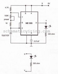
FLASH LIGHT ELECTRONIC DIAGRAM
IC NE555 works as an astable multivibrator with variation on the frequency. With this circuit, the LED blinks every half second. How long the blink time is, can be adjusted by adjusting the value of capacitor C1. Up to 18 additional LEDs can be attached to this circuit (36 LEDs total).
Components :
Diode D1-D2 : 5mm LED
Resistor R1 : 4K7 ohm
Resistor R2 : 1k ohm
Resistor R3-R4 : 330 ohm
Variable resistor VR1 : 100k ohm
Polar capacitor C1 : 10 uF/10 V
Capacitor C2 : 0.01 uF
IC1 : NE555
6V power supply
FAIRCHILD SEMICONDUCTOR FMS6418B ELECTRONIC DIAGRAM

FAIRCHILD SEMICONDUCTOR FMS6418B ELECTRONIC DIAGRAM
This part consists of a triple 6th order filter with selectable 33MHz or 8MHz frequencies. At any given time, the input signal’s DC levels must be between 0.0V and 1.3V to utilize the optimal headroom and to avoid clipping on the outputs. The 220 ?F capacitor coupled with the 150 ? termination forms a high pass filter that blocks the DC while passing the video frequencies and avoiding tilt. Lower values such as 10 ?F would create a problem. By AC coupling, the average DC level is zero. Thus, the output voltages of all channels will be centered around zero. Alternately, DC coupling the output of the FMS6418B is allowable. There are several trade-offs: The average DC level on the outputs will be 2V; each output will dissipate an additional 40mW nominally; The application will need to accommodate a 1V DC offset sync tip; And it is recommended to limit one 150 ? load per output.
SEMICONDUCTOR FMS6363 LOW COST VIDEO FILTER ELECTRONIC DIAGRAM

SEMICONDUCTOR FMS6363 LOW COST VIDEO FILTER ELECTRONIC DIAGRAM
The FMS6363 Low Cost Video Filter (LCVF) provides 6dB gain from input to output. In addition, the input will be slightly offset to optimize the output driver performance. The FMS6363 provides an internal diode clamp to support AC-coupled input signals. If the input signal does not go below ground, the input clamp will not operate. This allows DAC outputs to directly drive the FMS6363 without and AC coupling capacitor (usually 220 ?F). The offset is held to the minimum required value to decrease the standing DC current into the load.
CHALLENGES DESIGN OF SWITCHING LED ELECTRONIC DIAGRAM

CHALLENGES DESIGN OF SWITCHING LED ELECTRONIC DIAGRAM
The LED WEBENCH® online design environment predicts and simulates the response of an LED to constant current while taking into account several potential design parameters that are new to designers of traditional switching regulators.
AUDIO SCHEMATIC AND ROUTING ELECTRONIC DIAGRAM

AUDIO SCHEMATIC AND ROUTING ELECTRONIC DIAGRAM
It shows the connection and wiring between each parts and component of audio system of the vehicle such as the alternator, ignition switch, antenna meter, tail, audio, front speaker, rear speaker, tweeter speaker, and many more.
Friday, September 23, 2011
CONSTANT BRIGNESS LED AND MUTE CONTROL ELECTRONIC DIAGRAM

CONSTANT BRIGNESS LED AND MUTE CONTROL ELECTRONIC DIAGRAM
The output power of the modules are approximately 220W to 250W into 8? and 350W to 400W into 4?. Complete documentation for the amplifier modules can be found in the documents listed below. AN-1850 LME49830TB Ultra-High Fidelity, High-Power Amplifier Reference Design Although the power supply design is specific to the amplifier modules the concepts and circuit design may be used for any power supply purpose. The power supply is an unregulated design with an option to allow connection to either 120V or 240V mains. The design uses toroidal transformers, a fully integrated bridge, and various rail capacitors for ripple voltage reduction, noise suppression, and to act as high current reservoirs. Additional circuitry to control inrush current on power up and power up/ down Mute control are also included.
The topics discussed inside the application note including the introduction, overview, schematic and design, power supply, additional circuit, inrush current control, mute control, constant brightness LED circuit, summary, and many more.
NXP TDA3629 LIGHT POSITION CONTROLLER ELECTRONIC DIAGRAM

NXP TDA3629 LIGHT POSITION CONTROLLER ELECTRONIC DIAGRAM
schematic diagram of light position controller which is a monolithic integrated circuit often used in passenger cars. The potentiometer in the dashboard is used to define the light beam’s elevation of the car’s headlight to a state be the car driver.
ADJUSTABLE 1.5A STEP DOWN 1.5MHz SWITCHING REGULATOR ELECTRONIC DIAGRAM

ADJUSTABLE 1.5A STEP DOWN 1.5MHz SWITCHING REGULATOR ELECTRONIC DIAGRAM
However, an Adjustable 1.5A Step Down 1.5 MHz switching regulator circuit can also be used to overcome such problem. It uses ST1S03 step down DC-DC converter. The ST1S03 can also be used to power low-voltage digital core in HDD application .
With input voltage range 3V to 16V, the ST1S03 can gives current up to 1.5A. The circuit can use tiny surface-mount components due to an high switching frequency (1.5 MHz). Resistor divider is used to set the output voltage value. Components needed to build the divided are capacitors (2 pieces), schottky diode (1 piece), and inductor (1 piece).
5V DC REGULATED PHONE CHARGER ELECTRONIC DIAGRAM

5V DC REGULATED PHONE CHARGER ELECTRONIC DIAGRAM
Regulated phone charger which is used as an emergency charger for mobile phones with source from ordinary batteries, and works with 1.5V input DC voltage. At 5V, it can provide output to 70mA. If the current is drawn, the voltage will be drop. A006 microcontroller is used to create square wave which used to drive the Field Effect Transistor BBV93.
Thursday, September 22, 2011
PRECISION POWER REGULATOR ELECTRONIC DIAGRAM

PRECISION POWER REGULATOR ELECTRONIC DIAGRAM
A precision voltage source is quite easy, except when the voltage should be consistent over wide range of ambient temperature. This requirement might be needed in high precision measurement system environment. For example, to provide reference voltage in analog to digital conversion.
Li-Ion DRIVER WITH EXTERNAL PWM DIMMING ELECTRONIC DIAGRAM

Li-Ion DRIVER WITH EXTERNAL PWM DIMMING ELECTRONIC DIAGRAM
This boost converter is quite useful to improve conversion efficiency, reduce output ripple, and the use of small external components. In default, the LED current is set with external sensor resistor Rset, feed back voltage is regulated to 2000 miliVolts. During the operation, the current LED can be controlled using 1-wire digital interface through CTRL pin or with PWM signal that applied to the CTRL pin through the duty cycle. It determines the feedback reference voltage. The device also has a feature of integrated open LED protection that will disable the boost converter, this is to prevent the output from exceeding the absolute maximum ratings during open LED condition.
- L1: Murata LQH3NPN100NM0
- C1: Murata GRM188R61A105K
- C2: Murata GRM188R61E474K
- D1: ONsemi MBR0540T1
AUTOMATIC AIRFLOW DETECTOR ELECTRONIC DIAGRAM

AUTOMATIC AIRFLOW DETECTOR ELECTRONIC DIAGRAM
Sensor used in this circuit is a bulb filament. If there is no airflow, the filament resistance would give low value. On the other hand, if there is airflow, the filament resistance would varies. The variation of the resistance is caused by the heat difference between filament. It also effects to the voltage variation passing through that filament. That voltage difference will be processed by LM339 op-amp and displayed by the LED.
Parts list :
- LED1 : LED 5mm
- IC1 volt regulator : LM7805
- Polar Capacitor C1 : 47 uF/15V
- Resistor R1 : 100 ohm
- Resistor R2 : 470 ohm
- Resistor R3 : 10k ohm
- Potensiometer R4 : 100k ohm
- Resistor R5 : 1k ohm
- IC2 op-amp : LM339
- Bulb filament
- Power supply/battery 12V
AUTO RETRY fOR MAX1637 STEP-DOWN CONTROLLER ELECTRONIC DIAGRAM

AUTO RETRY fOR MAX1637 STEP-DOWN CONTROLLER ELECTRONIC DIAGRAM
On microprocessor supervisor (IC1), an internal power-fail comparator and manual-reset circuitry (MR) is included. IC1's PFI input will detect when Vout(1.8V) is above the internal reference voltage (1.25V). Active-low RESET and active-low SHDN go high after a timeout delay of 140ms, re-enabling IC2. The other way to re-enabling IC2 is when the supply voltage is first switched on : the 3.5V rail stabilizes after 140ms will cause active-low RST to go high and activate IC2.The active-low PFO output produces a pulse using the internal 60k pull-up resistor and external 0.1 uF capacitor if Vout falls below 1.25V (due to a short circuit, for instance).
Subscribe to:
Posts (Atom)